


Why Is Hybrid Inverter Pcb Important for Solar Systems?
A solar system may look simple from the outside. Inside, the Hybrid Inverter PCB controls a demanding energy conversation. It manages power from solar panels, batteries, household loads, and the electrical grid. Every transition requires accurate timing and stable protection.
The board carries power semiconductors, sensors, communication circuits, isolation barriers, and control processors. These parts work beside heat sources that may exceed 80°C during strong sunlight. A poor layout can increase electromagnetic interference, voltage stress, and conversion losses. Small design errors can become costly field failures.
Dr. Alex Lidow, a respected power-electronics expert, has said, “Power conversion is the heart of all electronics.” His observation explains why the Hybrid Inverter PCB deserves serious attention. It is not merely a connection platform. It is the inverter’s control and protection center.
Engineers typically examine creepage distance, thermal paths, grounding, surge protection, and component derating. They also test switching behavior under changing loads and battery conditions. Compliance with relevant safety and grid-interconnection requirements supports dependable deployment. Yet certification alone does not guarantee perfect field performance.
Real installations are less predictable. Dust, humidity, vibration, and uneven cooling can expose weaknesses that laboratory tests miss. A stronger PCB design uses clear fault handling and serviceable construction. Still, no design is flawless. Even experienced teams may underestimate aging connectors or software-driven thermal events.
That uncertainty makes verification essential. A reliable Hybrid Inverter PCB should protect people, preserve energy efficiency, and maintain stable operation over years. Its value becomes clearest when sunlight disappears, the battery is nearly full, and the home still needs power.
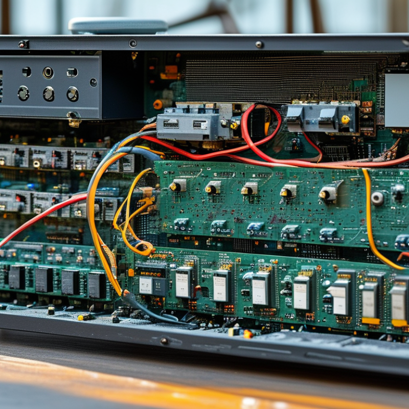
A hybrid inverter PCB is the control and power-routing board inside a hybrid inverter. It coordinates solar input, battery charging, grid exchange, and household loads. Unlike a basic inverter board, it must manage several energy paths at once. Sensors measure voltage, current, temperature, and insulation conditions. Gate drivers then control switching devices within milliseconds.
This role matters as solar systems become more complex. IRENA’s Renewable Capacity Statistics 2024 reported about 346 GW of new solar capacity added worldwide in 2023. Many of these systems need flexible storage and load control. A well-designed PCB helps maintain stable conversion when clouds pass, batteries change temperature, or loads suddenly start. It also supports communication, fault detection, relay control, and safe shutdown. Small details matter. A weak solder joint can create heat near a high-current connector.
In field inspections, thermal management often deserves more attention than it receives. Copper layers, heat paths, spacing, protective coatings, and connector quality all affect service life. The IEA PVPS Trends in Photovoltaic Applications 2024 report recorded global PV capacity above 1.6 terawatts by the end of 2023, increasing pressure on reliability and maintainability. Still, no PCB design is perfect. Higher switching speed may improve efficiency but increase electromagnetic noise. More protection can improve safety but add cost and response delay. Engineers must balance these compromises through testing, not assumptions.
A hybrid inverter PCB is the control and power-routing center of a solar system. It receives DC electricity from the solar array and battery. A microcontroller then reads voltage, current, temperature, and battery status. These measurements guide the switching circuit, which converts DC into stable AC power for household loads.
The process is continuous. Very fast power switches adjust their timing to produce the correct waveform. The PCB also manages maximum power point tracking, helping panels operate near their most productive voltage. When solar output changes, it can direct energy toward loads, battery charging, or grid interaction. In a well-designed board, isolated sensing circuits separate high-voltage paths from control signals. This reduces shock risks and protects sensitive components.
Protection happens in real time. Fuses, surge devices, current sensors, and temperature monitoring can respond to faults within milliseconds. During maintenance, technicians often inspect discolored connectors, cracked solder joints, and dust near cooling paths. These small details can reveal larger electrical or thermal problems. Heat remains the stubborn variable. Poor airflow may shorten component life, even when software appears normal. No PCB design is perfect; sensor drift, electromagnetic noise, and aging capacitors still require testing. Careful calibration and recorded performance checks make the system more dependable.
A hybrid inverter PCB acts as the system’s electrical control center. It manages energy from solar panels, batteries, the grid, and household loads. During field inspections, technicians often trace faults back to sensing or switching circuits. These small board sections influence the entire power flow.
The PCB controls high-speed switching devices that convert DC electricity into stable AC power. It also supports maximum power point tracking for changing sunlight conditions. Voltage and current sensors measure performance several thousand times per second. The controller then adjusts charging, discharging, and grid interaction. Protection circuits respond to overvoltage, overheating, short circuits, and abnormal current. Fast protection matters.
Communication circuits allow the inverter to exchange data with batteries, meters, and monitoring systems. Copper paths carry heavy current, while signal paths require careful separation. Designers also use insulation gaps, thermal interfaces, and heat dissipation structures. Poor layout can create noise, heat, or unreliable readings. A board may pass factory testing yet struggle in dusty, humid environments. That possibility deserves honest attention. Regular inspection of connectors, solder joints, and cooling areas helps identify early degradation. Technicians should also verify firmware settings and sensor accuracy during maintenance. Small measurement errors can gradually reduce charging efficiency or cause unnecessary shutdowns. In practical solar installations, PCB quality affects safety, service life, and daily energy availability.
A hybrid inverter PCB controls power between solar panels, batteries, the grid, and household loads. Its design directly affects efficiency and safety. IEA PVPS Trends 2024 reported about 447 GW of new solar capacity installed worldwide in 2023. More installations mean greater pressure on inverter reliability. A poorly routed PCB can increase switching losses, electromagnetic interference, and heat around power components. Small layout errors can become expensive failures.
Thermal design matters greatly. Copper thickness, creepage distance, ventilation, and component spacing must match the system’s voltage and current. IEC 62109-1 and IEC 62109-2 define safety requirements for power converters used in photovoltaic systems. These requirements are practical, not decorative. For example, insufficient clearance near a high-voltage connector may allow arcing during humidity or dust exposure. A stronger PCB also supports accurate battery charging and faster fault isolation.
Efficiency data can look impressive on paper. Fraunhofer ISE’s Photovoltaics Report 2024 shows modern photovoltaic systems continuing to improve conversion performance, but real installations face heat, vibration, and unstable loads. Engineers should test PCBs under repeated thermal cycling, not only at room temperature. This is often overlooked. A compact board may reduce material costs, yet restrict airflow and shorten capacitor life. Design reviews should question these trade-offs before production, because laboratory success does not always predict field reliability.
A hybrid inverter PCB is the system’s control center. It switches power between solar panels, batteries, loads, and the grid. IEA PVPS Trends 2024 recorded about 456 GW of new solar capacity in 2023, pushing global capacity beyond 1.6 TW. That scale makes PCB reliability a practical concern, not a laboratory detail.
Select a PCB around real operating conditions. Check maximum DC voltage, continuous current, surge rating, MPPT range, isolation, creepage, and clearance. Match the board with battery voltage and BMS communication. Thermal design deserves equal attention. A board may pass bench tests yet fail inside a 55°C cabinet. Look for heat spreading, fan control, capacitor temperature ratings, and humidity protection. EMC performance matters near radio equipment and long cable runs. Check compliance evidence against relevant grid and safety standards, not only a datasheet.
Maintenance starts with records. Log fault codes, temperatures, fan hours, battery events, and unusual restart patterns. Inspect connectors, solder joints, capacitors, and corrosion during scheduled service. Use a thermal camera when safe; a small hot spot can reveal loose terminals before damage spreads. Keep vents clear and tighten connections to the specified torque. Update firmware through controlled procedures. Do not ignore intermittent faults. They often become expensive faults. IRENA’s Renewable Capacity Statistics 2024 reported 345.5 GW of solar additions in 2023, although reporting methods differ from IEA PVPS. The difference is a useful reminder: field data is never perfectly clean. Review PCB performance after one season of heat, dust, and changing loads.
| Data Dimension | Typical Reference Data | Why It Matters in a Hybrid Solar Inverter | Selection Criteria | Maintenance and Inspection Points |
|---|---|---|---|---|
| PCB Functional Sections | Common sections include power conversion, battery charging, DC protection, AC switching, control logic, sensing, communication, and auxiliary power. | The PCB coordinates power flow between photovoltaic panels, batteries, household loads, and the utility grid. | Confirm that the board architecture supports the required operating modes: grid-tied, battery backup, off-grid, and solar priority. | Check connectors, relays, fuses, terminal blocks, and communication interfaces for discoloration, looseness, corrosion, or heat damage. |
| System Power Rating | Residential hybrid inverter systems commonly range from approximately 3 kW to 15 kW; larger commercial systems may be rated above 15 kW. | The PCB must carry the expected current without excessive temperature rise or electrical stress. | Match the PCB design with the inverter's continuous power, short-term overload capability, battery voltage, and maximum PV input power. | Inspect high-current paths for darkened copper, lifted pads, cracked solder joints, and abnormal heating during operation. |
| Battery Voltage Range | Typical battery buses include approximately 48 V for low-voltage battery systems and approximately 100–600 V for high-voltage battery systems. | Battery voltage determines insulation requirements, switching-device ratings, sensing accuracy, and protection design. | Verify compatibility with the battery chemistry, nominal voltage, maximum charge voltage, discharge limits, battery management system, and communication protocol. | Keep battery terminals tight and dry. Never work on the PCB while the battery and PV sources are energized. |
| Maximum DC Input Voltage | Many residential PV inputs are designed for several hundred volts DC. The exact limit depends on the inverter design and local installation conditions. | Excessive DC voltage can damage switching devices, capacitors, insulation, and measurement circuits. | Select a PCB whose voltage rating exceeds the calculated maximum cold-weather open-circuit voltage of the PV strings. | Check for insulation breakdown, carbon tracking, damaged surge components, and loose PV connectors after abnormal events or lightning. |
| Maximum PV Input Current | A typical residential MPPT input may support roughly 10–30 A per tracker, but the permitted value varies by inverter model and design. | Input-current limits protect PCB traces, fuses, inductors, connectors, and semiconductor switches from overload. | Compare the short-circuit current and operating current of each PV string with the PCB and inverter input limits, including applicable design margins. | Inspect DC terminals, current sensors, fuses, and inductors for hot spots or signs of sustained overcurrent. |
| MPPT Performance | Modern solar inverters commonly use one or more independent maximum power point trackers to accommodate different roof orientations and shading conditions. | Stable MPPT control improves energy harvest when irradiance and module voltage change throughout the day. | Consider the number of MPPT channels, MPPT voltage window, startup voltage, maximum current per tracker, and independent string support. | Review operating data for abnormal voltage fluctuations, repeated tracking faults, or a sudden drop in energy yield from one channel. |
| Switching Devices | Power PCBs may use MOSFETs, IGBTs, or other semiconductor switches selected according to the DC voltage, current, switching frequency, and topology. | Switching devices control conversion efficiency, thermal performance, noise, overload response, and long-term reliability. | Check voltage and current ratings, switching losses, thermal resistance, gate-drive compatibility, and the availability of qualified replacement parts. | Maintain clean heat-transfer surfaces and verify that fans, heat sinks, thermal pads, and temperature sensors operate correctly. |
| Capacitor Selection | DC-link and filtering circuits may use electrolytic, film, or ceramic capacitors. Lifetime is strongly affected by temperature, ripple current, and voltage stress. | Capacitors stabilize the DC bus, reduce ripple, and support reliable switching. Degradation can cause increased ripple, alarms, and converter failure. | Check capacitance, voltage rating, ripple-current rating, temperature rating, expected service life, and the capacitor's physical fit on the PCB. | Look for bulging, leakage, venting, discoloration, elevated ripple, or unusual acoustic noise. Replace only with parts meeting the original specifications. |
| Thermal Design | Electronic component life generally decreases as operating temperature rises. A commonly used engineering rule is that a 10°C increase can approximately double the reaction rate of many aging processes. | Effective heat dissipation limits semiconductor, capacitor, relay, and solder-joint stress. | Evaluate heat sinks, airflow paths, thermal sensors, fan control, enclosure ventilation, and the inverter's permitted ambient temperature range. | Keep ventilation openings clear, remove dust with approved methods, and record temperature alarms or repeated thermal derating. |
| PCB Materials and Construction | Power boards commonly use multilayer constructions with copper thickness selected according to current, temperature rise, and mechanical requirements. | Suitable materials improve insulation strength, current capacity, mechanical stability, and resistance to thermal cycling. | Review board thickness, copper weight, creepage and clearance, solder mask quality, conformal coating requirements, and thermal-via design. | Inspect for delamination, cracked solder joints, moisture residue, damaged coating, and contamination around high-voltage areas. |
| Electrical Protection | Common protection devices include fuses, circuit breakers, surge protective devices, pre-charge circuits, overvoltage protection, and overtemperature shutdown. | Protection reduces damage caused by short circuits, switching surges, lightning-induced transients, and abnormal operating conditions. | Confirm protective-device ratings, interruption capacity, coordination, grounding arrangement, and compatibility with the installation voltage. | Check protective indicators, replace operated fuses with the correct type, and investigate the cause before re-energizing the system. |
| Isolation and Safety Spacing | Required creepage, clearance, insulation, and dielectric withstand values depend on working voltage, pollution level, altitude, and applicable safety standards. | Adequate isolation helps prevent arcing, electric shock, fire, and control-side damage between high-voltage and low-voltage circuits. | Use a PCB evaluated for the target voltage and environment, with clearly separated power, control, communication, and protective-earth paths. | Do not bridge, scrape, drill, or modify isolation barriers. Test insulation only with procedures approved for the specific inverter. |
| Communication Interfaces | Common interfaces include CAN, RS-485, Ethernet, Wi-Fi, and dry-contact or digital-input connections. | Communication enables battery state reporting, remote monitoring, energy management, firmware updates, and coordinated shutdown. | Confirm protocol compatibility, isolation, connector type, cable length, termination requirements, and cybersecurity provisions. | Check communication cables, shielding, termination resistors, connectors, error logs, and firmware status without interrupting approved safety controls. |
| Environmental Protection | Outdoor inverter enclosures are commonly specified with an ingress-protection rating such as IP65 or a comparable level, depending on the product design. | Protection from dust, moisture, condensation, and salt mist helps prevent corrosion, leakage current, and insulation failure. | Match the PCB coating and enclosure protection to the installation location, humidity, pollution level, altitude, and coastal or agricultural conditions. | Inspect enclosure seals, cable glands, drain paths, condensation, corrosion, and signs of insects or water entry. |
| Efficiency and Standby Consumption | Well-designed solar inverters often achieve peak conversion efficiencies above 95%, while actual daily efficiency varies with load, temperature, battery operation, and operating mode. | Lower conversion losses reduce heat generation and improve usable solar and battery energy. | Compare efficiency curves rather than relying only on peak efficiency. Consider MPPT efficiency, battery charge/discharge efficiency, and standby use. | Compare long-term energy data with expected site conditions and investigate unexplained increases in nighttime or standby consumption. |
| Quality and Testing | Relevant evaluation commonly includes functional testing, thermal testing, insulation testing, electromagnetic-compatibility testing, and protection verification. | Testing reduces the risk of latent defects and verifies that the PCB performs safely under normal and abnormal conditions. | Request traceable test records, incoming inspection criteria, burn-in or load-test procedures, and documented revision control. | Keep maintenance records containing fault codes, test results, component replacements, firmware revisions, and inspection dates. |
| Recommended Maintenance Interval | Visual and environmental checks are commonly performed at least annually; dusty, humid, coastal, or high-temperature sites may require more frequent inspections. | Routine maintenance identifies airflow restrictions, loose connections, corrosion, and abnormal heating before major failure occurs. | Set the interval according to the manufacturer's service instructions, site conditions, operating hours, and local electrical regulations. | Isolate AC, PV, and battery energy sources using the approved shutdown procedure, then allow stored energy to discharge before qualified servicing. |
| Replacement and Repair Decision | A PCB should be repaired or replaced when it has repeated faults, burned conductors, damaged isolation barriers, failed protection circuits, or components that cannot be safely verified. | Correct decisions reduce downtime and prevent secondary damage to batteries, PV modules, loads, and grid-connected equipment. | Use a form-fit-function compatible board with matching hardware, firmware, ratings, connectors, protection features, and revision requirements. | Repairs should be performed only by qualified personnel using ESD controls, approved test equipment, and documented commissioning checks. |
| Key Selection Priorities | Electrical compatibility, thermal capability, environmental durability, safety protection, communication support, serviceability, and lifecycle cost. | A PCB that matches the complete system is more important than one selected only by nominal power rating or initial purchase price. | Use a technical checklist covering voltage, current, MPPT, battery interface, protection, cooling, standards, monitoring, warranty, and spare parts. | Reassess performance after major system changes, including battery expansion, PV-string modification, firmware updates, or changes in operating environment. |


For those larger-sized parts, or smaller quantity runs, we have 2 independent powder coat booths and ovens. The quality, durability and affordability of today’s powder coating finishes make this the process of choice for world-class companies.
Powder coating advantages over other forms of coating are many. Materials used in the Powder coating process can be metals and non-metals that come in a multitude of thicknesses, textures, colors, etc. Another of Powder coating’s biggest advantages over conventional coatings is its ability to create finishes in many different textures. Powder Coating Booths allow us the ability to apply these advantages to large products.
Tri-State Fabricators runs a full-service conveyor line for painting. Wet painting can provide protection or decoration to many different part styles. From start to finish, every project is easier to undergo random and point-based inspection by our skilled painting team.
Advantages to our Wet Paint Line are these lines start with product prep and ends with a thorough inspection of a high quality finished product. Our ability to complete large and small projects with a superior finish and doing so in a timely and economical fashion. This passes along the savings in production to our customers. When powder coating ins not an option, our Wet Paint Line gets the job done right the first time.
When the parts get big and heavy we roll-out our custom paint racks and oversize booth. By utilizing our partnerships with all the major paint brands, we can match virtually any color with wet paint.
The advantages of having access to a Wet Paint Booth are many. Large projects of many different shapes can be loaded into the booth. The Wet Paint Booth offers an environment that is much more controlled than a typical parts painting operation.
Not only are they used because of their controlled environment, but they’re are also advantageous when it comes to applying paint to parts that are needed in industries that require specialty coatings such as medical, aerospace, etc.
Our military forces have some very high standards when it comes to the finish of their vehicles and equipment. From the first pre-treatment step to final coat, it takes a great deal of knowledge and experience to protect the men and women of our armed forces. They deserve only the best, and Tri-State Fabricators provides it.
All of our processes are closely monitored by our staff and management teams. Both of which are highly trained in the processes of metal fabrication and finishing. Tri-State Fabricators’ goal is to always fully satisfy each and every customer, including the military. We will always put a 110% into what we do.
Abrasive media blasting is an excellent way to remove old paint, rust, and increase the paint/powder adhesion. Glass beads produce a much smoother and brighter finish than angular abrasives; leaving the part clean yet without any dimensional change. Chemically inert and environmentally friendly, we can recycle our beads approximately 30 times; making them a more preferred method of metal cleaning or surface finishing.
Advantages to Glass Bead Blasting are many. Glass bead blast media is used when a project is needing rough surfaces need to become smooth for applications of coatings such as paint. It is typically used to clean paint and rust from a product surface without deforming the surface it is being used on. Overall, compared to many other blasting media, Glass Bead Blasting is a very economical choice and those savings are always passed on to our customers.
Tri-State Fabricators utilize a zinc phosphate wash to clean and etch the material to ensure the best paint adhesion possible. The unique design of our 3-stage wash system does the work like a 5-stage. From Cleaning and rinsing to conversion coating and post-treatment, Our Part Washing process is a complete service and works throughout the fabrication service and the finishing service.
Along with the previously mentioned benefits, Curing is a vital chemical reaction that leaves the product finish hard and relatively safe from mild abrasion and aggressive corrosion. This process can be done in more than one way; ambient air-dry or in curing ovens at temps that exceed 240°.
From fixing paint mistakes (someone else’s of course) to simply cleaning our paint line hooks, our burn-off oven is put to good use. After a quick burn-off, a little clean up, and a fresh coat of paint, your parts will look better than new.
Why does our Burn-Off Oven work so well? Because super heating the air around parts turns the materials into ashes. From paint and powder coatings to rubber and machining oils, high temps do the job without degrading the integrity of the part.
Masking is a vital part of producing high quality products. We have die-cut masking patterns to protect machined surfaces as well as a wide range of plugs and caps to protect threaded holes and bolts. We provide permanent and temporary masking.
Masking allows the selected sections of a product to be protected from a fabrication or finishing service. This can be with both chemicals when etching and tapes, paints when only finishing just a section of the product. Masking is great in aiding the customization process of a project.
Screen printing is a photographic process that transfers artwork onto a porous nylon screen which allows colored ink to flow through the screen and be deposited on an aluminum or plastic component. We can generally have just about any design created onto a screen for your parts.
Some of the advantages of Screen Printing are, brand recognition for your business displaying on your products, assembly instructions, product warnings/hazards, etc. Tri-State Fabricators produces Screen Printing of the highest quality so you know it’s durable.
Metal Finishing is the art of treating the exterior portion of product, often metal but can also be made of other materials, so that the surface is clean and free of any debris. Then the process of applying coats or either paint of powder coat takes place. This coating process improves the quality of the product in both appearance and resistance to wear and corrosion.
Tri-State Fabricators, Inc., understands that a project typically isn’t complete until a high-quality finish has been added to your product. This is why our painting and powder coating teams continuously inspect the products throughout the Metal Finishing process.