

Choosing the right Silicon Inductor requires more than comparing inductance values on a supplier page. Designers must connect the component’s electrical behavior with the real circuit, board space, operating temperature, and production goals. A compact part may look ideal, yet its quality factor can fall at the target frequency. That difference can weaken filtering, matching, or signal integrity.
Practical evaluation should begin with the required inductance, frequency range, current level, and acceptable loss. Check impedance curves, self-resonant frequency, tolerance, and temperature stability. Package dimensions also matter. A 1.0 mm component can simplify placement, but it may demand tighter assembly control. Review the manufacturer’s datasheet, qualification reports, and recommended layout details. Independent laboratory measurements are valuable when specifications appear incomplete or unusually optimistic.
Bench testing often reveals details that calculations miss. Measure insertion loss with the intended substrate, connectors, and nearby components. Inspect performance after thermal cycling, not only at room temperature. No selection method is perfect. Parasitic coupling, fixture errors, and layout changes can distort results. I have seen a promising inductor fail because the evaluation board differed from the production stack-up. That mistake was avoidable, but not obvious at first. A reliable choice therefore balances simulation, verified measurements, supplier credibility, and realistic manufacturing conditions. This guide explains those decisions clearly, helping engineers compare Silicon Inductor options without treating one impressive specification as the whole answer.
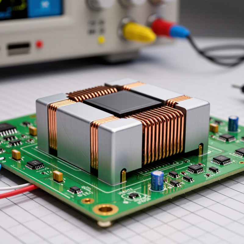
Choosing the right silicon inductor starts with understanding what it does. A silicon inductor is an integrated passive component formed within a semiconductor process. It stores energy in a magnetic field and resists rapid changes in current. In radio-frequency circuits, it can match impedance, tune oscillators, filter unwanted signals, or connect an antenna network. Its small footprint matters. So does its electrical behavior.
The core specifications deserve careful reading. Inductance sets the expected reactance at a target frequency. Quality factor indicates how much energy is lost, while self-resonant frequency marks where parasitic capacitance changes performance. Current handling and resistance also affect heating and signal loss. Measure under realistic temperature and frequency conditions. A room-temperature result may mislead. Layout is equally important; nearby metal, ground planes, and routing can shift the measured value.
For selection, match inductance, tolerance, Q value, and operating frequency to the circuit function. Check model accuracy before trusting simulation results. In practice, a network analyzer and controlled test fixture reveal details that a datasheet may hide. I would also compare two footprints, because a smaller part is not automatically better. That assumption fails surprisingly often. Leave design margin for process variation and temperature drift. Some choices remain imperfect when efficiency, size, and bandwidth conflict. Recheck the circuit after assembly, not only on paper.
| Selection Dimension | What It Means | Representative Silicon-Inductor Data | Selection Guidance |
|---|---|---|---|
| Primary Function | Defines how the inductor is used in the circuit. | RF matching, filtering, resonance, impedance transformation, and supply-noise isolation | Choose the component according to the circuit objective rather than inductance alone. A matching network may prioritize Q, while a power or bias network may prioritize current handling. |
| Inductance Value | The nominal opposition to changes in current, expressed in nanohenries for most integrated RF applications. | Approximately 0.5–100 nH; many RF designs use about 1–30 nH | Select the value required by the target frequency and matching topology. Confirm the effective inductance at the actual operating frequency. |
| Operating Frequency | The frequency range over which the component maintains acceptable electrical performance. | Commonly hundreds of MHz to several GHz | Use measured or modeled S-parameters at the intended frequency. Parasitic capacitance and substrate loss become increasingly important as frequency rises. |
| Quality Factor (Q) | The ratio of reactive energy to resistive energy loss; higher Q generally indicates lower loss. | Typically about 5–30 at RF, depending on frequency, geometry, and process | Choose a higher-Q device for narrowband matching, resonators, and low-loss filters. Moderate Q may be adequate for broadband matching or damping applications. |
| Self-Resonant Frequency (SRF) | The frequency at which inductive and parasitic capacitive effects resonate. | Often approximately 1–20 GHz for integrated RF structures | Keep the operating frequency comfortably below the SRF. Near or above SRF, the component may behave capacitively instead of inductively. |
| DC Resistance (DCR) | The resistance of the conductive path measured at or near direct current. | Approximately 0.1–10 Ω, depending on inductance, metal width, and layout | Lower DCR reduces conduction loss and voltage drop. Check the complete signal or bias path because substrate and metal losses also affect RF performance. |
| Current Handling | The current level that can be carried without excessive heating, electromigration risk, or unacceptable performance shift. | Often from several mA to a few hundred mA for integrated structures | Verify continuous and peak current separately. Integrated silicon inductors are generally intended for RF and signal applications, not high-current power conversion. |
| Tolerance | The allowed variation between the nominal inductance and the manufactured value. | Commonly around ±5% to ±20%, depending on process and design | Use tighter tolerance when the circuit has a narrow matching window. Include process, voltage, temperature, and layout variation in the design margin. |
| Temperature Stability | The degree to which inductance, Q, and resistance change over temperature. | Parameter drift is application- and process-dependent; resistance usually increases with temperature | For outdoor, automotive, or high-temperature systems, evaluate the full temperature range using validated models or measured data rather than room-temperature values only. |
| Substrate and Shielding | The silicon substrate and surrounding structures influence eddy-current loss, parasitic capacitance, and electromagnetic coupling. | Performance depends on substrate resistivity, metal stack, spacing, and optional shielding structures | Use a suitable substrate model and maintain the recommended keep-out area. Ground shields can reduce coupling but may also increase parasitic capacitance. |
| Physical Area | The die or layout area occupied by the inductor structure. | Typically from a fraction of 1 mm² to several mm² for on-chip RF inductors | Larger structures can improve inductance or Q but consume more area and may increase parasitic coupling. Optimize area together with electrical performance. |
| Equivalent Circuit Model | A model representing series resistance, inductance, substrate loss, and parasitic capacitance. | Common elements include Ls, Rs, Cp, and substrate resistance or capacitance | Use a frequency-dependent model for simulation. A simple ideal inductor model is usually insufficient for GHz circuits. |
| Layout Sensitivity | The effect of routing, ground proximity, neighboring metal, and via placement on electrical behavior. | Potentially significant at RF and microwave frequencies | Copy the validated layout conditions used in characterization where possible. Keep connections short, symmetric, and free from unnecessary metal near the inductor. |
| Best-Fit Application | The type of circuit where silicon inductors typically provide the greatest benefit. | RF transceivers, low-noise amplifiers, voltage-controlled oscillators, matching networks, and integrated filters | Use silicon inductors when compact integration and RF performance are more important than very high current capability or extremely low loss. |

How to Choose the Right Silicon Inductor?
Defining the Electrical Requirements for Your Application
Choosing a silicon inductor starts with the circuit, not the component catalog. Define the operating frequency, target inductance, acceptable tolerance, and required impedance. A 2.4 GHz matching network may need a small inductance with high Q, while a lower-frequency filter may prioritize stable inductance over peak performance. Write these values down.
Pay close attention to self-resonant frequency. The inductor should operate comfortably below this point, where its behavior remains predictable. Check Q at the actual working frequency, not only at a preferred test condition. Losses can reduce filter selectivity and increase signal attenuation. Temperature range matters too. Silicon characteristics and package parasitics can shift the response.
Current requirements deserve careful review. Integrated silicon inductors often suit low-power RF circuits, but they may not tolerate the current expected by power-conversion designs. Examine DC resistance, saturation behavior, and thermal limits in the technical data. Then verify the choice with a network analyzer and the intended PCB layout. A simulated match may change after routing.
My early selections relied too heavily on nominal inductance. That was a mistake. Measurement fixtures, ground paths, and nearby copper influenced the result more than expected. Leave margin for tolerance and layout variation, and question every assumption before releasing the design.
Typical inductance starting ranges for common RF and mixed-signal applications
Silicon inductors are commonly selected in the low-nanohenry range. Use the operating frequency, required inductance, quality factor, self-resonant frequency, and loss budget to refine the initial range. The final value should be verified with electromagnetic models and measured in-circuit because layout and substrate effects can significantly change performance.
How to Choose the Right Silicon Inductor?
Comparing Key Silicon Inductor Specifications
Choosing a silicon inductor starts with its inductance value, but that number rarely tells the whole story. Check the tolerance, because a listed 10 nH part may vary significantly across production and temperature. In RF matching networks, even a small shift can move the circuit away from its target frequency. Measure it.
Quality factor, or Q, shows how efficiently the inductor stores energy. A higher Q usually reduces loss, but only at a specific frequency and test condition. Compare Q at your actual operating frequency, not only the headline value. The self-resonant frequency must also stay comfortably above that frequency. Near resonance, parasitic capacitance can change the component’s behavior.
Direct-current resistance affects heat and efficiency, especially in power-related designs. Check the rated current, temperature rise, and saturation behavior together. A low resistance value may look attractive, yet it may not reflect performance under real load. Silicon inductors can also respond differently to temperature, layout, and nearby metal structures. Use the recommended land pattern, then verify results on the assembled board. Datasheet comparisons can be misleading. I have seen excellent simulated results weaken after packaging and routing were included. Consider package size, frequency range, voltage limits, and measurement conditions before making a final choice.
Choosing a silicon inductor requires more than checking inductance and resistance. Package geometry can change magnetic coupling, pad parasitics, and heat flow. A compact package saves board space, but its smaller copper path may increase current density. IPC-2221C and IPC-2152 offer practical guidance for conductor spacing and current capacity. Use them before finalizing the footprint.
Layout deserves careful attention. Keep the inductor away from noisy switching nodes and sensitive signal traces. Minimize the loop area between the inductor, capacitor, and power switch. JEDEC JESD51 standards also remind engineers that thermal performance depends on the complete board, not only the package. For example, a 0.5 W loss with 40°C/W thermal resistance creates about a 20°C temperature rise. That margin can disappear inside a crowded enclosure. My early layouts often underestimated nearby copper temperature. That mistake was expensive to correct.
Tips: Compare package-level and board-level thermal data. Measure the hottest pad with a calibrated thermocouple. Check clearance after assembly, not only in CAD. Leave copper around thermal pads when the datasheet permits it. Recheck performance at maximum ambient temperature and load. A smaller package may appear efficient, but airflow, copper area, and neighboring components can change the result. Use measured prototypes to challenge simulation assumptions; simulations are useful, but they are not always right.
Selecting and validating a silicon inductor requires more than comparing nominal inductance values. Start with the circuit’s operating frequency, current range, voltage swing, and available area. A 10 nH device may look suitable, yet its quality factor can fall sharply near the target frequency. Check inductance tolerance, series resistance, self-resonant frequency, and saturation behavior.
Measure real performance under realistic conditions. Use an impedance analyzer or calibrated network analyzer to verify inductance and Q across temperature. Test the component on the intended circuit board, not only on a reference fixture. Copper width, ground spacing, and nearby metal can change the result. Keep the layout consistent.
Watch the current carefully. Silicon inductors often trade compact size for higher loss and limited current handling. Record insertion loss, thermal rise, and output ripple during normal operation. A thermal chamber can reveal drift that room-temperature tests miss. It is easy to overlook substrate coupling.
I once trusted a simulation that used ideal coupling. The prototype disagreed. That mistake changed my validation process. Compare at least two qualified structures, repeat measurements, and document every fixture and calibration step. If efficiency drops after assembly, investigate the board before rejecting the inductor. The best option is the one that remains predictable in the finished system.


For those larger-sized parts, or smaller quantity runs, we have 2 independent powder coat booths and ovens. The quality, durability and affordability of today’s powder coating finishes make this the process of choice for world-class companies.
Powder coating advantages over other forms of coating are many. Materials used in the Powder coating process can be metals and non-metals that come in a multitude of thicknesses, textures, colors, etc. Another of Powder coating’s biggest advantages over conventional coatings is its ability to create finishes in many different textures. Powder Coating Booths allow us the ability to apply these advantages to large products.
Tri-State Fabricators runs a full-service conveyor line for painting. Wet painting can provide protection or decoration to many different part styles. From start to finish, every project is easier to undergo random and point-based inspection by our skilled painting team.
Advantages to our Wet Paint Line are these lines start with product prep and ends with a thorough inspection of a high quality finished product. Our ability to complete large and small projects with a superior finish and doing so in a timely and economical fashion. This passes along the savings in production to our customers. When powder coating ins not an option, our Wet Paint Line gets the job done right the first time.
When the parts get big and heavy we roll-out our custom paint racks and oversize booth. By utilizing our partnerships with all the major paint brands, we can match virtually any color with wet paint.
The advantages of having access to a Wet Paint Booth are many. Large projects of many different shapes can be loaded into the booth. The Wet Paint Booth offers an environment that is much more controlled than a typical parts painting operation.
Not only are they used because of their controlled environment, but they’re are also advantageous when it comes to applying paint to parts that are needed in industries that require specialty coatings such as medical, aerospace, etc.
Our military forces have some very high standards when it comes to the finish of their vehicles and equipment. From the first pre-treatment step to final coat, it takes a great deal of knowledge and experience to protect the men and women of our armed forces. They deserve only the best, and Tri-State Fabricators provides it.
All of our processes are closely monitored by our staff and management teams. Both of which are highly trained in the processes of metal fabrication and finishing. Tri-State Fabricators’ goal is to always fully satisfy each and every customer, including the military. We will always put a 110% into what we do.
Abrasive media blasting is an excellent way to remove old paint, rust, and increase the paint/powder adhesion. Glass beads produce a much smoother and brighter finish than angular abrasives; leaving the part clean yet without any dimensional change. Chemically inert and environmentally friendly, we can recycle our beads approximately 30 times; making them a more preferred method of metal cleaning or surface finishing.
Advantages to Glass Bead Blasting are many. Glass bead blast media is used when a project is needing rough surfaces need to become smooth for applications of coatings such as paint. It is typically used to clean paint and rust from a product surface without deforming the surface it is being used on. Overall, compared to many other blasting media, Glass Bead Blasting is a very economical choice and those savings are always passed on to our customers.
Tri-State Fabricators utilize a zinc phosphate wash to clean and etch the material to ensure the best paint adhesion possible. The unique design of our 3-stage wash system does the work like a 5-stage. From Cleaning and rinsing to conversion coating and post-treatment, Our Part Washing process is a complete service and works throughout the fabrication service and the finishing service.
Along with the previously mentioned benefits, Curing is a vital chemical reaction that leaves the product finish hard and relatively safe from mild abrasion and aggressive corrosion. This process can be done in more than one way; ambient air-dry or in curing ovens at temps that exceed 240°.
From fixing paint mistakes (someone else’s of course) to simply cleaning our paint line hooks, our burn-off oven is put to good use. After a quick burn-off, a little clean up, and a fresh coat of paint, your parts will look better than new.
Why does our Burn-Off Oven work so well? Because super heating the air around parts turns the materials into ashes. From paint and powder coatings to rubber and machining oils, high temps do the job without degrading the integrity of the part.
Masking is a vital part of producing high quality products. We have die-cut masking patterns to protect machined surfaces as well as a wide range of plugs and caps to protect threaded holes and bolts. We provide permanent and temporary masking.
Masking allows the selected sections of a product to be protected from a fabrication or finishing service. This can be with both chemicals when etching and tapes, paints when only finishing just a section of the product. Masking is great in aiding the customization process of a project.
Screen printing is a photographic process that transfers artwork onto a porous nylon screen which allows colored ink to flow through the screen and be deposited on an aluminum or plastic component. We can generally have just about any design created onto a screen for your parts.
Some of the advantages of Screen Printing are, brand recognition for your business displaying on your products, assembly instructions, product warnings/hazards, etc. Tri-State Fabricators produces Screen Printing of the highest quality so you know it’s durable.
Metal Finishing is the art of treating the exterior portion of product, often metal but can also be made of other materials, so that the surface is clean and free of any debris. Then the process of applying coats or either paint of powder coat takes place. This coating process improves the quality of the product in both appearance and resistance to wear and corrosion.
Tri-State Fabricators, Inc., understands that a project typically isn’t complete until a high-quality finish has been added to your product. This is why our painting and powder coating teams continuously inspect the products throughout the Metal Finishing process.